Photolithography: Sub-micron level resolution ultraviolet contact lithography capabilities
Suss MJB3 mask aligner (1 mm – 3” diameter substrates)
Canon PLA501F mask aligner (2” – 4” wafers)
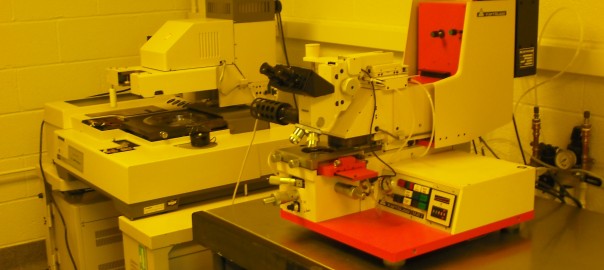
E-beam Lithography: Dedicated scanning electron microscope (SEM) for e-beam lithography, resolution allows writing of sub-100 nm features.
Lithography Support:
Laurell Technology WS-400 spin coater with fragment adapter (4” x 4” max. substrate size)
Positive and negative photoresists, MMA and PMMA e-beam resist