Sample Cleaning
- Novascan PSDP-UV8T UV Ozone System: UV-ozone cleaner with substrate heating
- Plasma Etch PE-100-RIE Plasma cleaner and reactive ion etcher
Physical Vapor Deposition
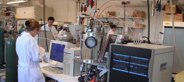
- DV-502A Turbo High Vacuum Evaporator
The e-beam evaporator uses an electron beam produced by a charged tungsten filament under high vacuum to melt a target anode. Atoms from the target evaporate and proceed to coat everything in line of sight with a thin layer of the anode material.
- Plasma Sciences Automated Research Coater
The sputter system uses an electromagnet to focus high energy Ar ions onto the target, thus ejecting target material from the source to the substrate. This instrument is used to deposit thin films including indium tin oxide and aluminum.
- Angstrom Engineering Evovac Deposition System
The Evovac consists of 5 sources; 2 resistive sources,2 sputter sources and an electron beam source. The resistive and electron-beam sources can be run simultaneously, allowing the codeposition of up to 3 materials. The system is equipped with a sample stage heater capable of heating the sample holder plate to 600 degrees Celsius.
Chemical Deposition
- Spin coater with fragment adapter
Spin coating involves dissolving a material of interest in a solvent, and then spinning to achieve a uniform, defect-free film. The MORE Center has Laurell Technologies spin coaters located in the glovebox, benchtop and clean room, allowing for the deposition of a variety of materials, including air sensitive polymers and photoresist.
Miscellaneous
- Ulvac-Riko Mila 5000 Rapid Thermal Annealer
Rapid thermal annealing is the application of high heat to semiconductors, ferroelectrics and other thin film devices to repair defects, and to improve mechanical and electrical properties. The sample is housed inside an o-ring sealed transparent quartz protective tube that maintains sample cleanliness. The RTA heats at rates up to 50°C/s, and can anneal at temperatures up to 1200°C. Vacuum, hydrogen/nitrogen, hydrogen/argon and pure nitrogen gases are available for the annealing environment.
- Kulicke & Soffa 4123 Wire Bonder
The wire bonder allows the user to to precisely apply a tiny lead for electrical contact under a microscope . The lead is welded to the conductor using ultrasound. The small wires are used to contact small semiconductor devices.